
photoelectric effect
In 1839, Edmond Becquerel discovered the process of using sunlight to produce an electric current in a solid material. But it took more than another century to truly understand this process. Scientists eventually learned that the photoelectric effect caused certain materials to convert light energy into electrical energy at the atomic level.
The photoelectric effect is the basic physical process by which a photovoltaic (PV) or solar cell converts sunlight into electricity. When light shines on a solar cell, it may be reflected, absorbed, or pass right through. But only the absorbed light generates electricity.
The energy of the absorbed light is transferred to electrons in the atoms of the solar cell. With their newfound energy, these electrons escape from their normal positions in the atoms of the semiconductor photovoltaic material and become part of the electrical flow, or current, in an electrical circuit. A special electrical property of the PV cell – a built-in electric field – provides the force, or voltage, needed to drive the current through an external load, such as a light bulb.
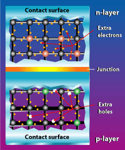
To induce the built-in electric field within a solar cell, two layers of somewhat differing semiconductor materials are placed in contact with one another. One layer is an n-type semiconductor with an abundance of electrons, which have a negative electrical charge. The other layer is a p-type semiconductor with an abundance of holes, which have a positive electrical charge.
Although both materials are electrically neutral, n-type silicon has excess electrons and p-type silicon has excess holes. Sandwiching these together creates a p-n junction at their interface, thereby creating an electric field.
When n- and p-type silicon come into contact, excess electrons move from the n-type side to the p-type side. The result is a buildup of positive charge along the n-type side of the interface and a buildup of negative charge along the p-type side.
Because of the flow of electrons and holes, the two semiconductors behave like a battery, creating an electric field at the surface where they meet – the p-n junction. The electrical field causes the electrons to move from the semiconductor toward the negative surface, where they become available to the electrical circuit. At the same time, the holes move in the opposite direction, toward the positive surface, where they await incoming electrons.