
thin film solar cell
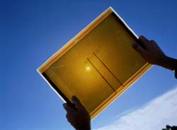
Thin-film solar cell.
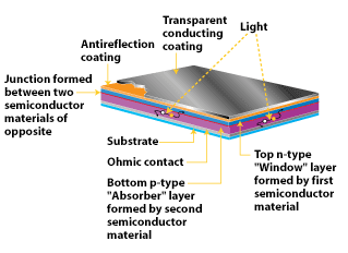
Polycrystalline thin-film cells have a heterojunction structure, in which the top layer is made of a different semiconductor material than the bottom semiconductor layer. The top layer, usually n-type, is a window that allows almost all the light through to the absorbing layer, usually p-type. An "ohmic contact" is often used to provide a good electrical connection to the substrate.
One scientific discovery of the computer semiconductor industry also has great potential in the photovoltaic (PV) industry: thin-film technology. The "thin film" term comes from the method used to deposit the film, not from the thinness of the film: thin-film cells are deposited in very thin, consecutive layers of atoms, molecules, or ions. Thin-film cells have many advantages over their "thick-film" counterparts. For example, they use much less material – the cell's active area is usually only 1 to 10 micrometers thick, whereas thick films typically are 100 to 300 micrometers thick. Also, thin-film cells can usually be manufactured in a large-area process, which can be an automated, continuous production process. Finally, they can be deposited on flexible substrate materials.
Thin-film deposition
Several different deposition techniques can be used, and all of them are potentially less expensive than the ingot-growth techniques required for crystalline silicon. We can broadly classify deposition techniques into physical vapor deposition, chemical vapor deposition, electrochemical deposition, or a combination. And like amorphous silicon, the layers can be deposited on various low-cost substrates (or "superstrates") such as glass, stainless steel, or plastic in virtually any shape.
In addition, these deposition processes can be scaled up easily, which means that the same technique used to make a 2-inch × 2-inch laboratory cell can be used to make a 2-foot × 5-foot PV module – in a sense, it's just one huge PV cell. Thin films are unlike single-crystal silicon cells, which must be individually interconnected into a module. In contrast, thin-film devices can be made as a single unit – that is, monolithically – with layer upon layer being deposited sequentially on some substrate, including deposition of an antireflection coating and transparent conducting oxide.
Thin-film cell structure
Unlike most single-crystal cells, a typical thin-film device doesn't have a metal grid for the top electrical contact. Instead, it uses a thin layer of a transparent conducting oxide, such as tin oxide. These oxides are highly transparent and conduct electricity very well. A separate antireflection coating might top off the device, unless the transparent conducting oxide serves that function.
Polycrystalline thin-film cells are made of many tiny crystalline grains of semiconductor materials. The materials used in these polycrystalline thin-film cells have properties that are different from those of silicon. So, it seems to work better to create the electric field with an interface between two different semiconductor materials. This type of interface is called a heterojunction ("hetero" because it is formed from two different materials, in comparison to the "homojunction" formed by two doped layers of the same material, such as the one in silicon solar cells).
The typical polycrystalline thin film has a very thin (less than 0.1 micron) layer on top called the "window" layer. The window layer's role is to absorb light energy from only the high-energy end of the spectrum. It must be thin enough and have a wide enough bandgap (2.8 eV or more) to let all available light through the interface (heterojunction) to the absorbing layer. The absorbing layer under the window, usually doped p-type, must have a high absorptivity (ability to absorb photons) for high current and a suitable band gap to provide a good voltage. Still, it is typically just 1 to 2 microns thick.
Copper indium diselenide
 |
| CuInSe2
|
Copper indium diselenide (CuInSe2 or "CIS") has an extremely high absorptivity, which means that 99% of the light shining on CIS will be absorbed in the first micrometer of the material. Cells made from CIS are usually heterojunction structures – structures in which the junction is formed between semiconductors having different bandgaps. The most common material for the top or window layer in CIS devices is cadmium sulfide (CdS), although zinc is sometimes added to improve transparency. Adding small amounts of gallium to the lower absorbing CIS layer boosts its bandgap from its normal 1.0 electron-volts (eV), which improves the voltage and therefore the efficiency of the device. This particular variation is commonly called a copper indium gallium diselenide or "CIGS" PV cell.
Cadmium telluride
Cadmium telluride CdTe) is another prominent polycrystalline thin-film material. With a nearly ideal bandgap of 1.44 eV, CdTe also has a very high absorptivity. Although CdTe is most often used in PV devices without being alloyed, it is easily alloyed with zinc, mercury, and a few other elements to vary its properties. Like CIS, films of CdTe can be manufactured using low-cost techniques.
Also like CIS, the best CdTe cells employ a heterojunction interface, with cadmium sulfide (CdS) acting as a thin window layer. Tin oxide is used as a transparent conducting oxide and antireflection coating. One problem with CdTe is that p-type CdTe films tend to be highly resistive electrically, which leads to large internal resistance losses. A solution is to allow the CdTe layer to be intrinsic (that is, neither p-type nor n-type, but natural), and add a layer of p-type zinc telluride (ZnTe) between the CdTe and the back electrical contact. Although the n-type CdS and the p-type ZnTe are separated, they still form an electrical field that extends right through the intrinsic CdTe. When it comes to making CdTe cells, a wide variety of methods are possible, including closed-space sublimation, electrodeposition, and chemical vapor deposition.
Thin-film silicon
The term "thin-film silicon" typically refers to silicon-based PV devices other than amorphous silicon cells and single-crystalline silicon cells (where the silicon layer is thicker than 200 micrometers). These films have high absorptivity of light and may require cell thicknesses of only a few micrometers or less. Nanocrystalline silicon and small-grained polycrystalline silicon – considered thin-film silicon – may be able to replace amorphous silicon alloys as the bottom cell in multijunction devices. As with other thin films, advantages include the savings of material, monolithic device design, use of inexpensive substrates, and manufacturing processes that are low temperature and possible over large areas.