MICROMACHINES AND NANOTECHNOLOGY: The Amazing New World of the Ultrasmall - 2. Computers, Crystals, and Chips
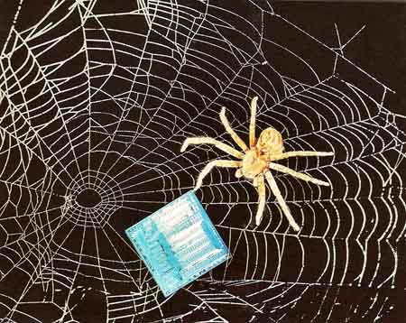
Figure 1. A complete, special-purpose computer can be formed on a silicon chip smaller than an ordinary spider.
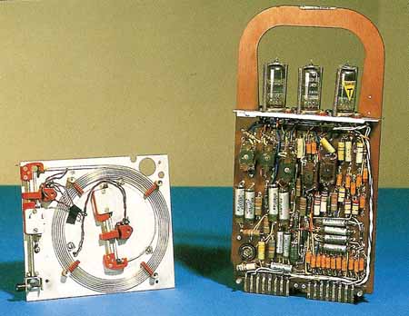
Figure 2. Glass triodes and other large components, such as these from a computer of 1960, have now been replaced by small silicon chips containing many millions of components.
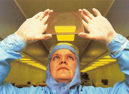
Figure 3. A worker checks a mask to be used in the manufacture of silicon chips.
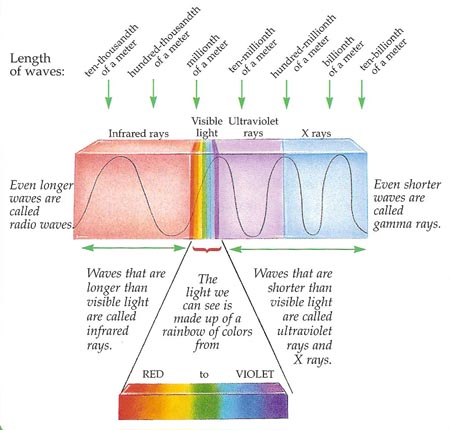
Figure 4. Visible and invisible light. The light we can see is just a small part of a complete spectrum of waves that also includes infrared rays, ultraviolet rays, and X-rays.
If you are sitting at home or at school reading this, you are probably surrounded by dozens, or perhaps even hundreds, of MICROCHIPS (see Figure 1). They are hidden away inside TVs, hi-fis, wrist-watches, computers, calculators, kitchen appliances, and many other modern gadgets. They help to control the latest car engines and passenger aircraft.
A microchip is also known as an INTEGRATED CIRCUIT. It is made from a single crystal of a substance called SILICON. The crystal is no bigger than your little fingernail and thin enough to pass through the eye of a needle. On the surface of this sliver of silicon, a complicated pattern of tiny electronic components and connecting pathways has been laid down.
Microchips are the most advanced products of miniaturization yet made. Their story began roughly a century ago.
The Dawn of Electronics
When a piece of metal is heated in empty space – a vacuum – the metal gives off a stream of particles called ELECTRONS. Think of electrons as being the tiniest possible packets of electricity. A flow of electrons, therefore, creates an electric current. If you imagine moving electricity to be like water flowing over a waterfall, electric current is equivalent to the amount of water that goes over the waterfall each second.
In 1904 an English scientist, John Fleming, found a simple way to control an electron flow. He invented the DIODE. Built from two pieces of metal, known as electrodes, inside a vacuum-filled glass tube, the diode let current pass through only in one direction. The flow of electrons from the first electrode, which was hot, could be stopped or started depending on the voltage on the second electrode. If you think again of a flow of electricity as being like a waterfall, then voltage is equivalent to the height of the drop.
In 1906 an American scientist, Lee de Forest, took Fleming's idea a step further with his invention of the TRIODE. By placing a third, wire-mesh, electrode between the other two, de Forest was able to control the amount of current passing through the device. Very small changes in the voltage on the third electrode would cause big changes in current across the tube. This fact made triodes very useful as electronic components – devices that regulate a flow of electricity. Later they found their way into radio receivers, phonographs (record players), and television sets.
Switched On
Scientists also realized that triodes could work as switches. In other words, they could be made to flip from "on" (when a current passes through them) to "off" (when no current passes through). This was very important because switches are the most vital parts needed inside computers. Sets of switches can be used to represent instructions and information (see Figure 2).
In the late 1940s the first electronic computers were built using triodes. One of the earliest, called ENIAC, contained 18,000 triodes and weighed 30 tones! These computers were marvels of their age, but they suffered from some major problems.
Triodes are bulky, use a lot of power, and become hot when working. Computers made from them filled whole rooms, used a great deal of electricity, and had to be cooled by big fans. They were always breaking down, too, since each triode had a fairly short life.
Breakthrough
In 1947 three American scientists, William Shockley, John Bardeen, and Walter Brittain, invented an important new electronic device. It worked just like a triode but was solid, small, and needed very little power. The invention was a TRANSISTOR.
To work as an electronic switch, a transistor did not have to be heated. Instead, it relied on the special electrical properties of a SEMICONDUCTOR. This is a substance whose ability to pass a current improves as tiny amounts of impurities, known as DOPANTS, are added to it. The first transistors were built from a semiconductor called germanium. Eventually, however, silicon became the main semiconductor from which transistors and other electronic components were made.
Different parts of a crystal of silicon can be set up to act in the same way as the electrodes in a triode or a diode. This change is made by adding various tiny amounts of dopants to the silicon, such as boron in one region and phosphorus in another region. The result is a device that is small, stays cool, and last for a very long time.
In the 1950s transistors began replacing triodes as the basic building blocks of all computers. As a result, computers quickly shrank in size and became more dependable. Because they were smaller, information could travel around them more quickly, so computers also increased in speed.
At the same time, people began to realize all the different ways in which small, reliable computers might be applied. The space age had just begun, and computers were needed aboard spacecraft. But before they could be used for such tasks, computers would have to be reduced still further in size.
The Quarter-Inch-Square Marvel
Scientists began to ask: Instead of making components like transistors one at a time, why not make many of them together on the same crystal of silicon? The result would then be an integrated circuit – or a silicon chip.
In 1960 the first chip was made in the United States. Within a few years, chips containing several dozen transistors and other components were being manufactured. By 1975 the record stood at about thirty thousand components per chip. Because each component was now microscopic in size, the chips on which they were made became known as microchips. By 1994 it was possible to place over three million components on a single piece of silicon about a quarter-of-an-inch square.
In order to make a modern microchip, one draws a plan of all the components and connections. This plan is reduced in size hundreds of times, trough a series of photographs, until it is only about five or ten times bigger than the actual chip. From the miniaturized plan of the chip, a template, or mask, is created.
Fire and Light
Wafers of pure silicon are sliced from a rod-shaped crystal and put into a red-hot furnace. The heat causes the wafers to produce a thin outer layer of silicon dioxide – a substance through which electricity cannot flow. Then the wafers are taken out of the furnace and coated with a type of chemical known as a polymer. The particular kind of polymer used in microchip manufacture is soft and sensitive to light.
A coated wafer is carefully positioned under the mask containing the details of the chip to be manufactured. Ultraviolet light is shone through the mask and focused by an arrangement of lenses so that it forms a tiny, sharp image of the circuit pattern on the light-sensitive polymer. Ultraviolet light is used because the waves that make up ordinary light are too far apart to pick out the very fine details on a modern chip. In ultraviolet light the waves are closer together and so can produce a sharper outline through the mask (see Figure 3).
After the first exposure, the wafer is moved to a slightly different position so that another tiny region can be exposed to the ultraviolet light shining through the mask. In this way many copies of the chip are formed from one silicon wafer.
The Acid Test
The exposure of the polymer to light changes the polymer's solubility – the ease with which it can be dissolved by a special chemical. This chemical is known as a developer and is used to remove the polymer in the regions where it has been exposed.
The remaining polymer is baked to make it chemically resistant, and then the whole wafer is bathed in acid. Where the polymer has been dissolved, the acid is able to attack the underlying silicon dioxide and so expose the silicon below. As a result, the pattern of exposed silicon exactly matches the details contained on the mask.
Tiny amounts of different dopants are put onto the exposed silicon, at specific points. In this way, regions of the chip are formed that will work as diodes, transistors, and other components. Finally, very thin aluminum pathways are laid down to provide electrical connections.
Modern microchips may have ten or more different layers of components and connections. All the manufacturing stages just described must be repeated to produce each of the circuit layers. This mean the chips must go back into the furnace to begin the whole process again and again.
Challenges of Tomorrow Chips
For a number of years scientists have been asking: How much more can chips be miniaturized? Today's most advanced chips contain several billion transistors. At some point, researchers are likely to run up against problems that prevent a further reduction in size.
Already, microchips produce more heat for their area than the hotplate of an electric over. Since the chips would fail if they became too hot, cooling systems are needed that can remove heat as fast as it is produced. In the future, a limit may be reached on how quickly excess heat from chips can be carried away.
Another problem arises from excessive electrical effects. The voltage across a single transistor is quite small, but it occurs across such a tiny distance that it amounts to an extremely steep voltage drop. Such a voltage drop produces a powerful electrical effect in its immediate neighborhood. As the components on a chip are crowded closer and closer together, the electrical effects they give rise to may become so large that they prevent the transistors from working properly.
Many other difficulties confront the chip manufacturers of tomorrow. Perhaps the biggest challenge of all will be to find ways to create the ever-tiner components and pathways on the chip's surface. Its fineness of detail is limited by the size of the waves that are used to shine on the mask. Ordinary light has already been replaced by ultraviolet light (see Figure 4). Now even the limits of ultraviolet rays are being reached, and some scientists believe that the next generation of integrated circuits will have to make use of X-rays, which consist of even shorter waves.
Limits to the miniaturization of chips may eventually be reached, but not, scientists believe, before you will be able to carry a computerized copy of all the books in the Library of Congress around in your pocket.
| Superspeed Silicon?
How can computers and other electronic devices be made even faster and more powerful than they are today? One way is by miniaturizing the components on a silicon chip still further. This would reduce the distances that signals have to travel and so increase the speed with which information can be handled. An alternative approach is to look for new materials through which electrical signals can move faster.
A basic limit to the speed of a computer is the rate at which its transistors can flip from "off" to "on" and back again. Some scientists are investigating materials in which this so-called switching speed is much higher than it is in pure silicon. One of the new possibilities that are looking at is an alloy of silicon and germanium. New transistors made from a silicon-germanium alloy have been shown to switch on and off about three times faster than the fastest silicon transistor ever made. Researchers are now experimenting with ways to incorporate these superspeed switches into practical circuits. |